ICON Touch – Building a New touch-and-High-value STN display
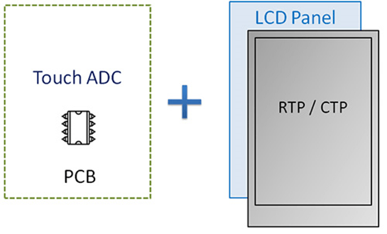
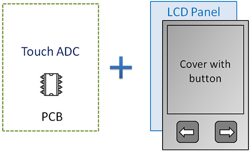
Nowadays, the STN-LCD display products equipped with touch functions are the most commonly adopted 3-in-1 structure as a combination of driving module circuit board(PCB), STN-LCD display, and resistive touch panel (RTP) or the capacitive touch panel (CTP). As Image 1 shows, few may use the integrated structure of driving module circuit board (PCB), STN-LCD display, and membrane switch, as shown in Image 2.
[Image 2]
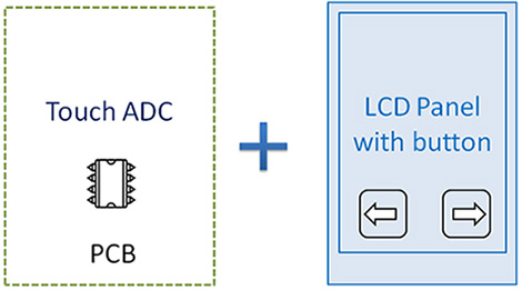
Winstar has come up with a new design concept: combining a driving module circuit board (PCB) and STN-LCD display as a 2-in-1 structure. The touch button is designed within the viewing area (VA) of LCD to increase the touch sensibility, as Image 3 shows.
[Image 3]
Feature of product:
(1) Applicable LCD: TN/STN/FSTN/VATN
(2) Operating Voltage:2.2V~5.5V
(3) ICON reacting to I/O port directly; moreover, with selectable active levels – Low or High.
(4) Low cost, simple structure.
(5) Support Multiple Touch ADC ICs.
(6) Low power consumption when in standby mode.
(7) Connection of external capacitor is available for touch sensitivity adjustment.
(8) Different types of IC selections, such as multi-touch or single touch are optional. Customers can choose the preferred one depending on the requirements.
(9) Automatic change-over standby mode/ operation mode.
(10) Auto-calibration feature. IC can calibrate automatically to get the standard value.
(11) PCB + PIN design is workable for a larger size STN-LCD display module.
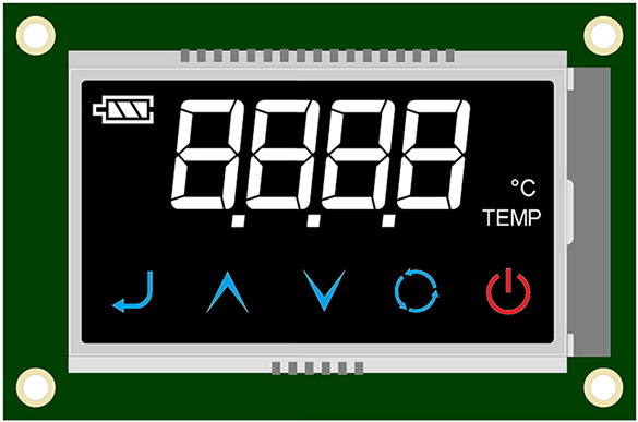
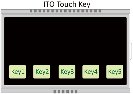
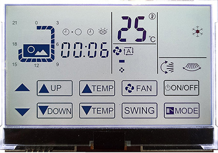
As shown in image 4, this is an ICON type STN-LCD display module with a capacitive touch button to elaborate this design further. The upper area of LCD is where ICON patterns are controlled by the controller or driver IC for the purpose of ICON graphics demonstration.
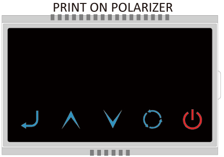
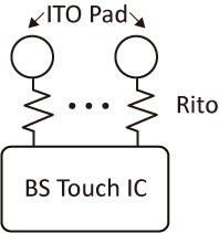
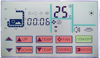
There are 5 color patterns in the lower area of the LCD. Silkscreen printing technology is used on these icons, and all icons are equipped with capacitive touch buttons. The structure of buttons is the transparent conductive ITO layers shaped like a rectangular block onto glass made for sensor pad functions, as shown in Image 5. There is a polarizer on the top of sensor pads with fixed images and color silkscreen printing, as Image 6 indicated. When laminating, the polarizer with fixed images shall precisely align with the rectangular block of transparent ITO layers. For positive image LCD products, the silkscreen printing is used in the lower polarizer; as for negative image LCD products, the silkscreen printing is used in the upper polarizer. After printing, it requires attaching a transparent protective film on the top of the polarizer to protect printings that may peel off by touching.
Considering the signal connection between the driving module circuit board (PCB) and STN-LCD display, the design utilizes pinned connections. Using ICON capacitive touch to design a touch sensor pad is a good option. Therefore, the display selection is not limited to size, and customers can choose a larger size of the display module. However, please note that in this kind of design for larger size, the touch sensor pad and ICON positions must be staggered and cannot overlap.
[Image 4]
 [Image 5]
|
 [Image 6]
|
When designing ICON Touch STN-LCD display products, the following requirements shall be taken into consideration.
(1) Dimension of the Touch Key:
The touch key can be designed in any shape. Considering human factors, it is generally designed with a rectangular shape. The sensitivity of the touch key is related to the size and thickness of the ITO sensor pad. The larger the sensor pad is, the higher the sensitivity of the touch key is. However, when the dimension of the ITO sensor pad surpasses finger sizes, the effect of increasing the sensor pad area for improving sensitivity will be limited. The ideal dimension of the ITO sensor pad is approximate 8~15mm, whereas it is suggested not to be smaller than 8x8mm to prevent sensor failures.
(2) The Distance between the Touch Keys:
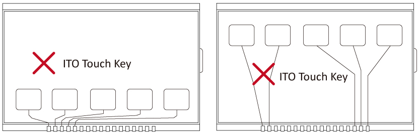
The application with multiple touch keys must keep a certain distance between the sensor pads to avoid any interferences. The minimum gap is suggested to keep larger than 2mm, as shown in Image 7.

[Image 7]
(3) Layout and Circuit Design of the Touch Key
Matching the circuit resistance and driver IC of the touch screen is crucial. The lower the circuit resistance is, the easier the adjustment of touch screen sensitivity will be. On the contrary, the adjustment of the touch screen sensitivity is more restricted or even cannot reach the expectation when the circuit resistance is higher. Take Image 8 as an example; the resistance (Rito) of the ITO is much higher than conducting wire
According to Ohm’s law, shorter or wider conducting tracks have less resistance; however, it may cause touch malfunction when the conducting track is too wide, and the touch sensitivity adjustment will become harder. Therefore, the circuit design is better be kept shorter, decreasing the negative impacts from possible unfavorable factors. On the other hand, the resistance must be ensured to reach the threshold of touch signal communication when considering a smaller conducting track.
[Image 8]
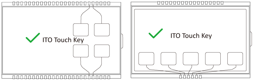
When designing the signal circuit layout, it is ideal for keeping all of the length and resistance the same to keep the sensing signal stable and consistent. An ideal layout is to keep the ITO sensor pad outside of the LCD viewing area and closer to the pin-out area (which means the closet area to the interface). Image 9 demonstrates an ideal circuit layout example. Take Image 10 as an example illustrating inappropriate layout design. This kind of layout may cause an unstable touching signal easily; the designer shall be better to avoid it.
[Image 9]
[Image 10]
Furthermore, regarding small-sized STN-LCD display products with touch functions, such as ICON displays smaller than 4.6-inch or Graphic type displays smaller than 3.5-inch, Winstar builds a more efficient solution by choosing a driver IC with display and touch functions, bonding it directly onto the STN-LCD panel, which is called COG (chip on glass). See the COG STN-LCD display designs in Images 11 to 13. For example, the blue mark is the display area of silkscreen printing, the green mark with silkscreen printing applied is the touch button, and the red mark is the icon displaying area and touch button.
This solution is highly integrated; it integrates the original ADC-Touch function and display function into the COG IC and eliminates the need for a driver PCB board and touch panel. The display function and touch function of the STN-LCD display can be combined into one COG IC, which also eliminates the need for display IC and touch IC. The advanced COG technology can effectively shorten the distance from the signal path to the driver IC and improve touch and display performance.
Winstar owns an advanced and professional COG production line manufacturing, which can provide customers with fast and high-quality OEM/ODM service to meet their product needs. We provide one-stop integrated solutions and OEM/ODM services that can shorten the developing phase of custom designs, effectively reduce the cost, enhance the value of customers’ products, and improve the competitiveness of customers’ products. Winstar builds a rock-solid quality.
[Image 11 COG STN-LCD]
[Image 12]
[Image 13]
If you want more information or if you have any questions, please contact Nijkerk Electronics!